We seek to unlock the transformative potential of integrated photonics.
We are enabling rapid, fabrication-tolerant photonic integrated circuit development for any wavelength or platform.
Our Partners
Our Mission
Our mission is to help unlock the valuable photonics markets by using design technology to enable new applications and reshape the inefficient and fragmented productisation cycle into an integrated and rapid process, analogous to the development of modern semiconductors.
Our Story
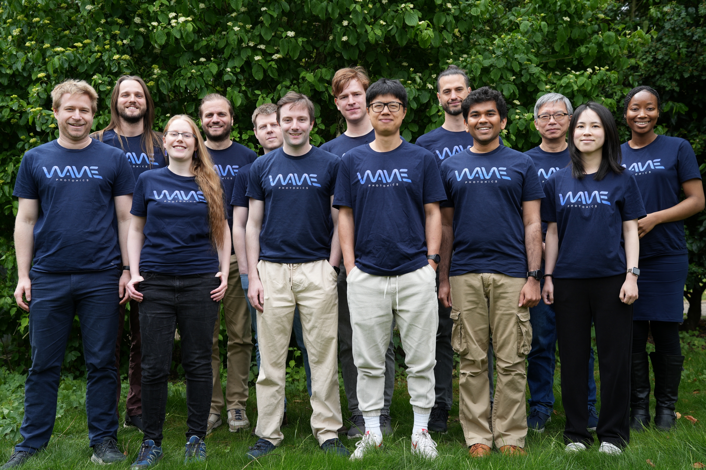
Wave Photonics is a Cambridge-based integrated photonics company offering photonics IP, products and services.
Wave Photonics was founded in May 2021 by James Lee and Matthew Anderson, two Cambridge Quantum Photonics PhDs, and Mateusz Kubica (CTO), a former quantitative finance VP with 10 years' experience in mathematical and computational modelling.
Integrated photonics uses the same scalable process used to make semiconductor electronics chips to make circuits for light. It’s being used as the platform for energy-efficient communications for AI and data centres, wearable healthcare sensors, rapid diagnostic tools, optical tensor processors, on-chip lidar, quantum technologies and a host of other transformative applications. However, in contrast with the mature semiconductor chip process, taking a photonic integrated circuit (PIC) from a concept to mass production is long and often prohibitively expensive.
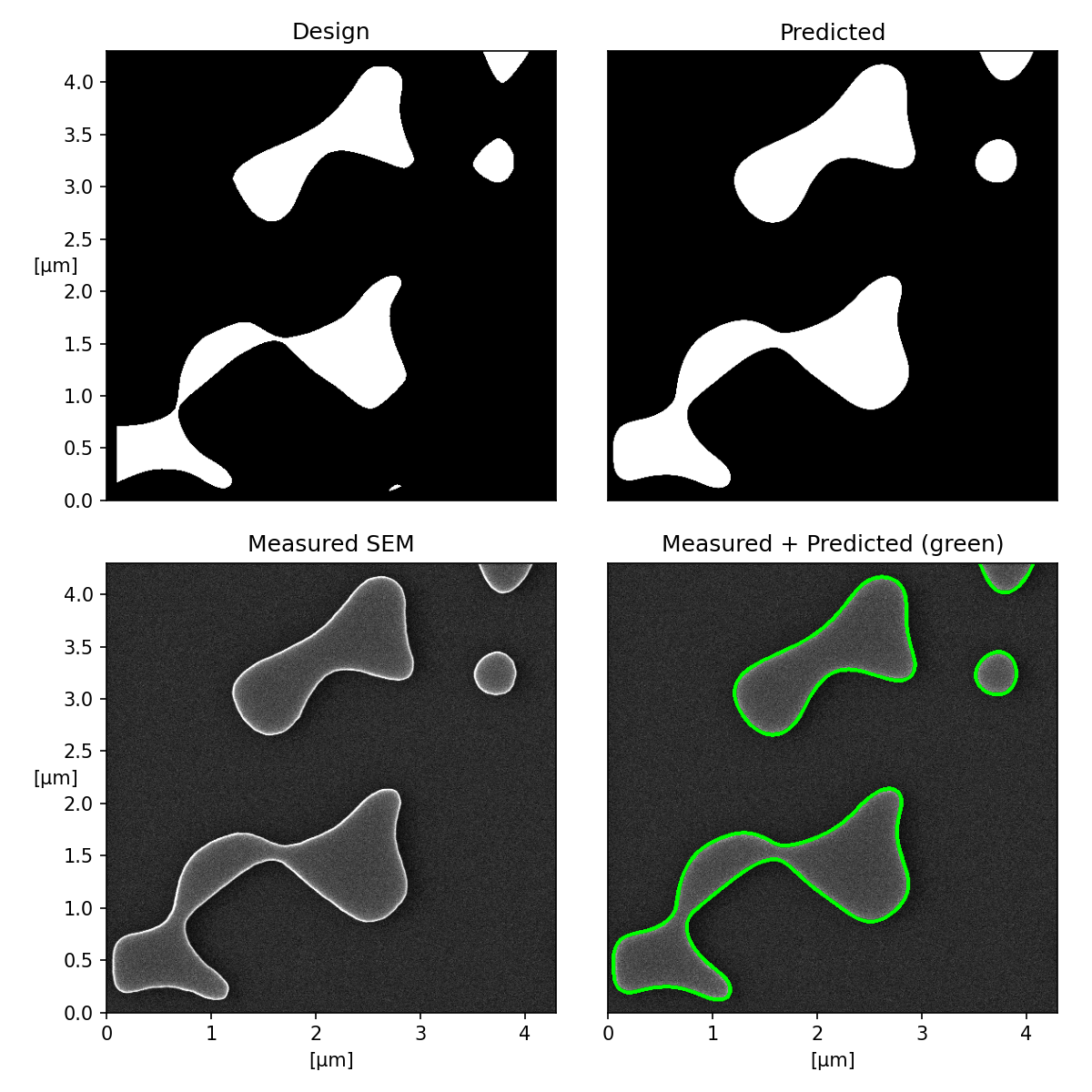
The three founders thought that statistics/optimisation could be used to improve integrated photonics. Since its founding, the company has built and validated its core computational photonics design technology to reduce photonic product development time and aims to use it to unlock the transformative potential of integrated photonics.
We’re located in Cambridge, UK, and are backed by great investors in the US and Europe, We’re also contributing to multiple projects funded by Innovate UK, the UK's innovation agency.
We have a talented team with backgrounds spanning integrated photonics, high-performance computing, quantum photonics, statistics, optimisation, technology consulting and semiconductors.
Our range of products and services can enrich and speed up the PIC development process.
Custom PDK Development
Our proprietary design technology enables us to design a custom or application-specific PDK in weeks. We can create state-of-the-art PDKs for any target material or wavelength to fast-track development for customers working on datacoms, sensing and quantum technologies.
Our PDK Management Platform provides a platform to digitally manage PDKs and streamline the designer experience by ensuring PDKs work with leading EDA tools, and provides ready-calculated S-parameters for circuit simulation.
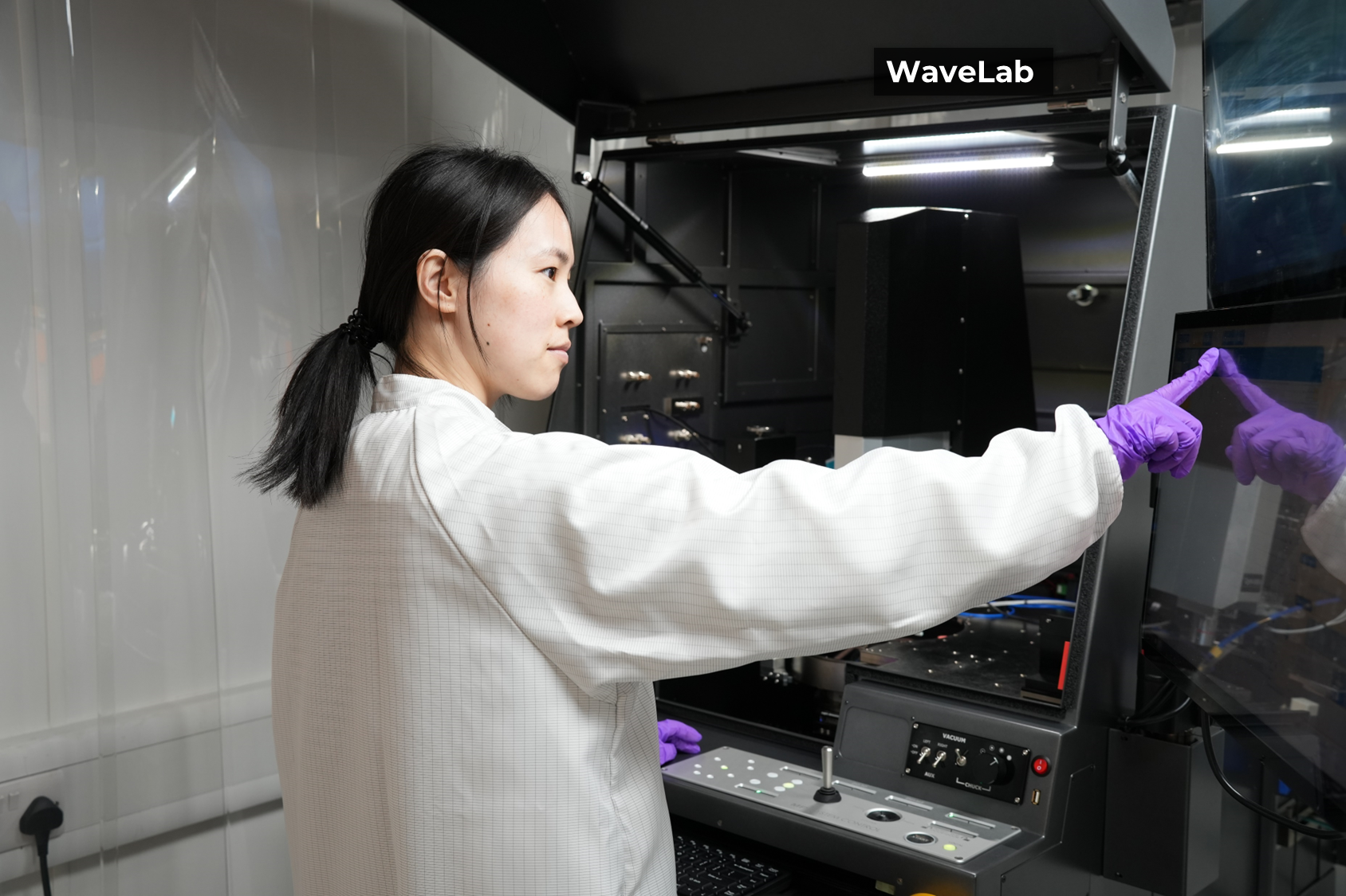
Our team of photonics and modelling experts offer custom PIC architecture development, chip design, and can manage the fabrication and characterisation process.
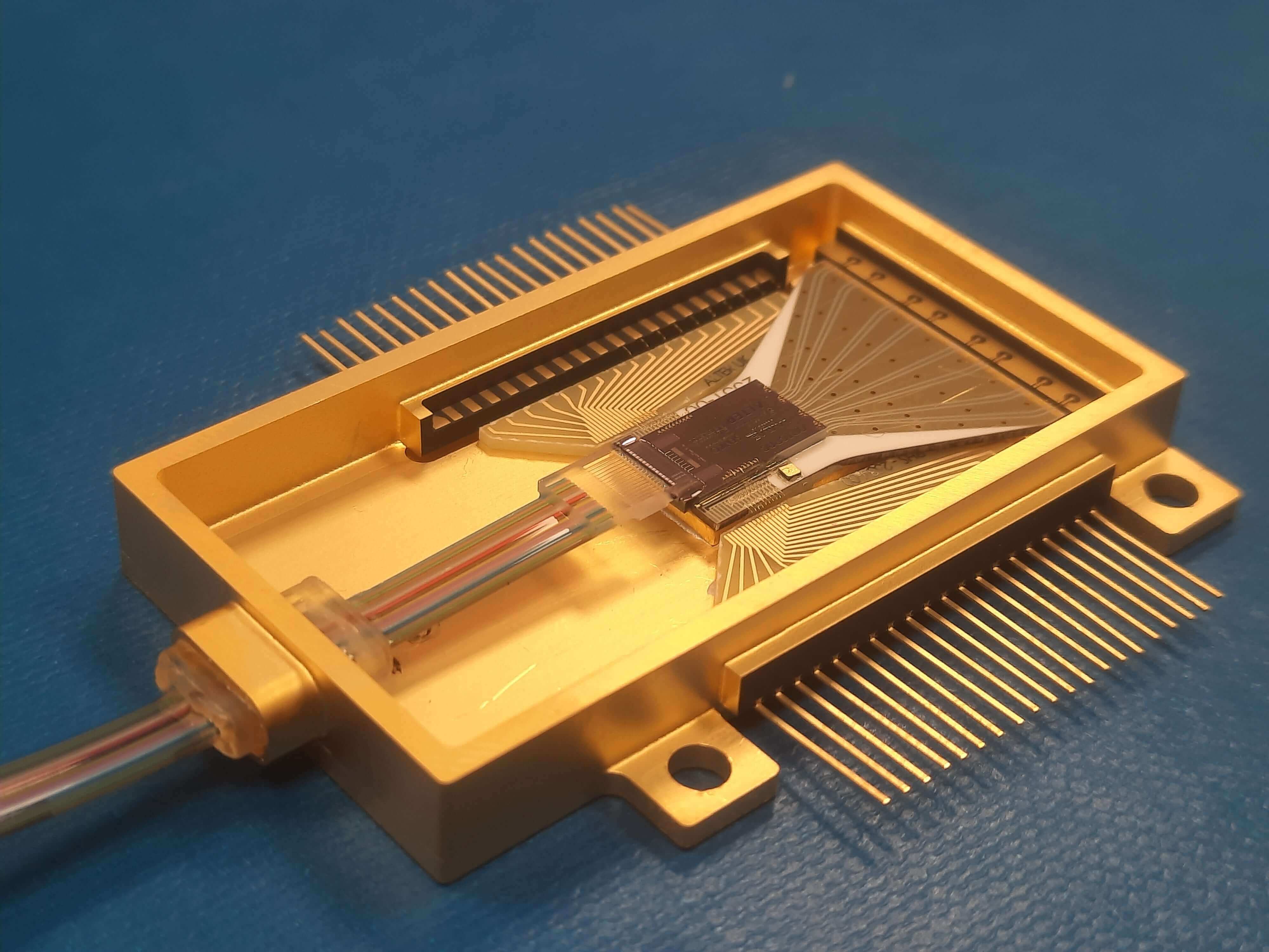
We offer easy-to-use reusable packaging templates which minimise custom development requirements and costs. With our QPICPAC offering, you can have packaged chips in as little as one month.
Component Libraries and Co-Packaged Optics (CPO) IP
Our IP consists of ready-to-go photonic components, energy-efficient modulator designs, driving and control circuits, and equaliser circuit designs. Our IP is available for licencing and can be accessed through other means.
We are backed by great investors in the US and Europe, including Berkeley Skydeck, Plug and Play, the UK Innovation & Science Seed Fund, Cambridge Enterprise Ventures, Redstone, QAI Ventures’ Quantum Fund, Kyra Ventures, Deep Tech Labs and several angel investors.
We enable rapid, fabrication-tolerant PDK development. Explore our offerings for your next integrated photonics product and reduce your PIC development time.
Find out more about our PDKs for your PIC applications.


.JPG)