Our PDK Management Platform provides a platform to digitally manage PDKs and streamline the designer experience by ensuring PDKs work with leading EDA tools. The platform automatically generates S-parameters for circuit simulation.
Our PDK Management Platform provides automatic compatibility with EDA tools, black-box IP protection, PDK version control, and hosted PDK access.
Automatic EDA compatibility
We ensure foundry PDKs are pre-packaged for leading design platforms with no manual setup or labeling required. Foundry users can download PDKs, integrate the PDK into their chosen EDA tool and start designing.
S-parameter generation
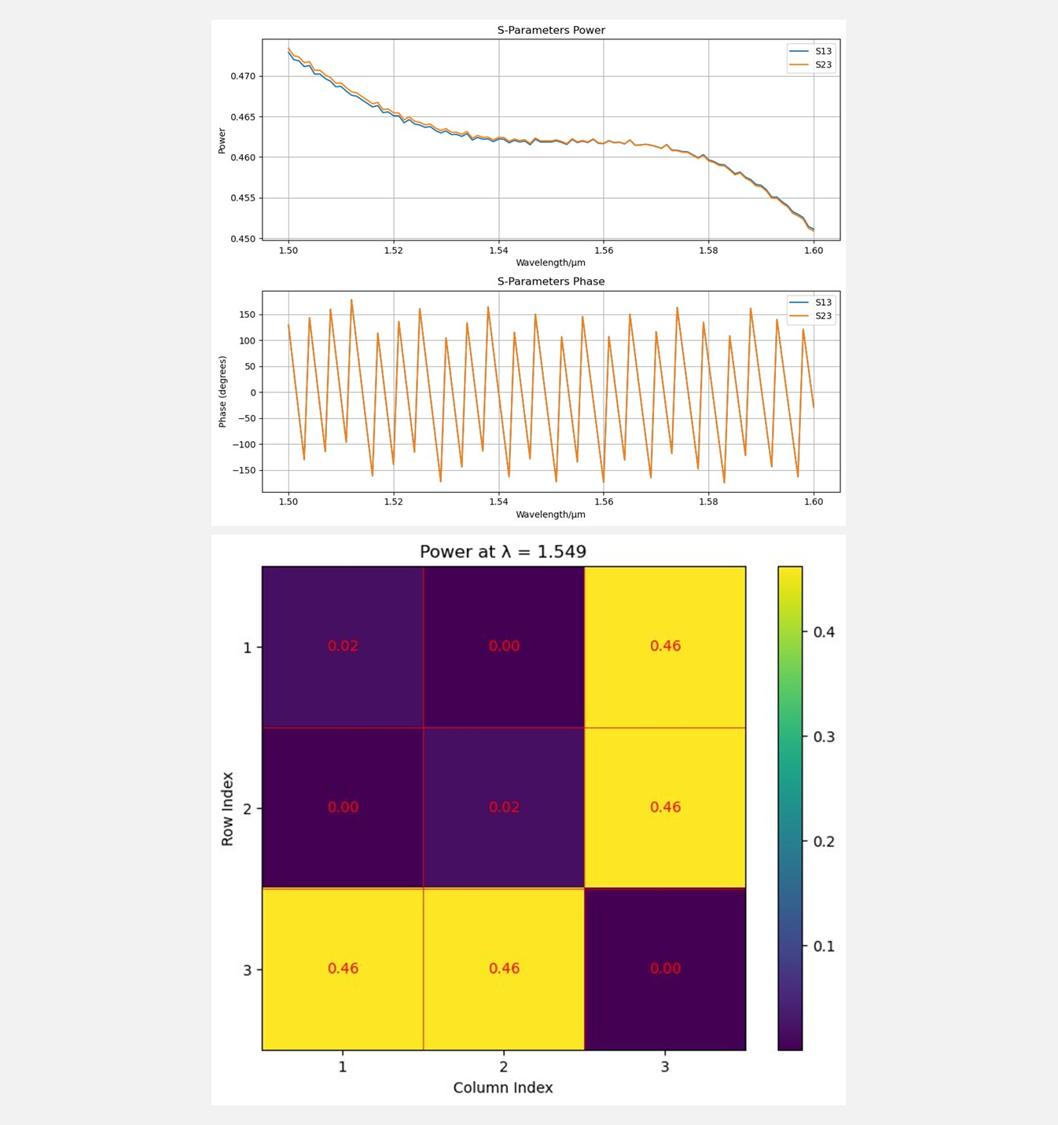
Scattering parameters (S-parameters) are generated using Wave Photonics’ built-in simulation engine. Fabrication-aware S-parameters allows foundry users perform full circuit simulation before taping out a chip. Using our fabrication model, S-parameters can also account for fabrication imperfections.
NDA tracking and black-boxing for IP protection and IP reuse
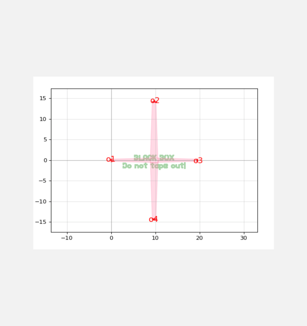
Foundries and other users can have secure design reuse and licensing without exposing critical IP. We obscure sensitive designs with black boxes to protect foundry and third-party IP, while still enabling visual circuit inspection. NDA tracking ensures PDKs are only shared with approved partners.
Automatic documentation
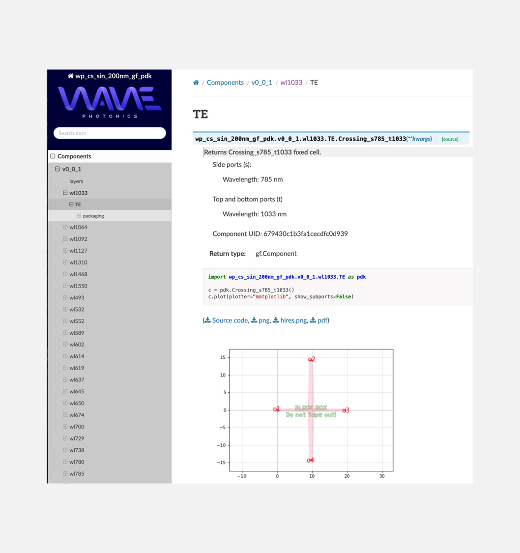
Documentation is automatically generated for the PDKs, ensuring users always have access to searchable, up-to-date and complete documentation. PDK and tool versions are tracked, avoiding mix-ups and accidental cross-use of conflicting PDKs.
With our PDK Management offering, commercial foundries can improve the customer experience by shortening design times and providing access to multiple EDA tool integrations.
01
Enable Wider Customer Adoption
Access to multiple EDA tool integrations
02
Shorter design time
Faster time to design and tapeout for foundry customers
03
Lowers support efforts
Free up time for higher-value work
04
Enhanced Security
Secure IP and data control through access permissions
Benefits for Research and Academic Foundries
Academic and research foundries can increase exposure of their fabrication process to industry and enhance collaboration with other organisations.
01
Boost Group Productivity
Organised and tracked designs enhance group productivity
02
Exposure to Industry
A streamlined route to open your fabrication process to industry and achieve wider impact
03
Enhanced Collaboration
Facilitate collaboration with the university and with other organisations - maximise academic impact
04
IP Exploitation
IP re-use facilitates IP licensing and exploitation
Case Study: CORNERSTONE PDK Management Platorm
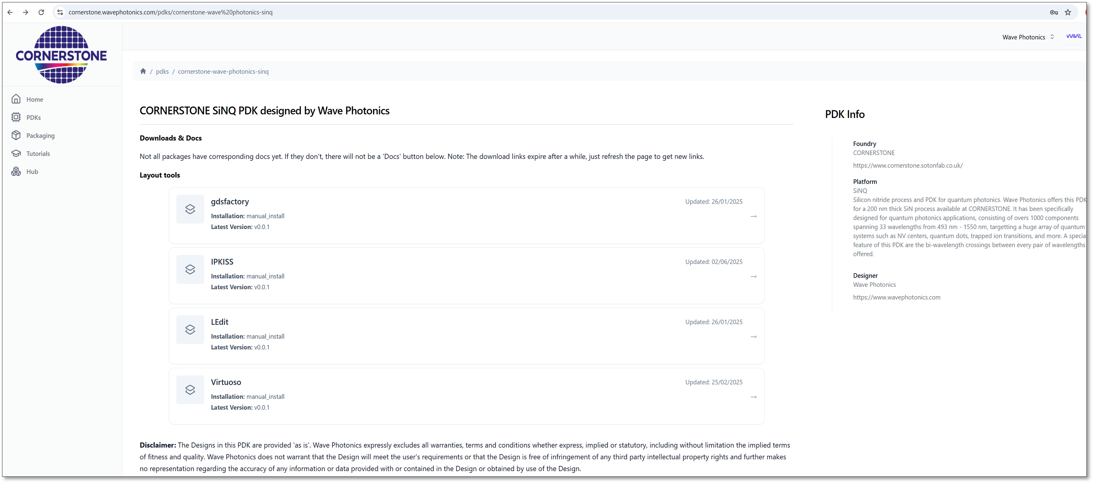
Wave Photonics supports CORNERSTONE, a UK-based open-source silicon photonics rapid prototyping foundry, to provide a platform for its users to access PDKs integrated into major EDA tools. CORNERSTONE users can now use CORNERSTONE PDKs with ready-calculated S-parameters for circuit simulation. See it here: cornerstone.wavephotonics.com
Creating and maintaining foundry PDKs can be a lengthy process, especially when managing multiple technology platforms, as we do at CORNERSTONE. Wave Photonics’ PDK Management Platform greatly reduces the workload of keeping our existing PDKs up to date and integrating new ones into EDA tools. This collaboration enables us to focus more on enriching our open-source component libraries while enjoying the simplicity and efficiency of this innovative approach.
Dr. Emre Kaplan
PDK Manager, CORNERSTONE, University of Southampton
PDKs packaged for multiple EDA tools - including GDSFactory, IPKISS, L-Edit, and Virtuoso - with support for Synopsys and Latitude Design Systems coming soon
Users can download PDKs, and access documentation with one click
Each version is tracked with clear release history and metadata
PDK management workflow
From upload to hosting: foundries can automate documentation, simulation, and access control in one seamless pipeline. To find out more, get in touch with us at info@wavephotonics.com.
Upload PDKs
Use a template to define PDKs in a compatible format.
01
PDKs are processed
We run S-parameters, generate documentation and package for EDA tools.
02
Hosting
New version of PDKs available to customers with NDA tracking and fine-grained access control.
03
Continuous Processing
All new PDKs uploaded are continuously processed and available to foundry users.
We enable rapid, fabrication-tolerant PDK development. Explore our offerings for your next integrated photonics product and reduce your PIC development time.
Find out more about our PDKs for your PIC applications.


.JPG)


