
Product Overview
We offer access to component designs, the information required to design a photonic chip, a reusable turnkey packaging solution for prototyping and R&D, as well as integrated photonics fabrication process setup at target wavelengths.
Explore our product offering
Integrated Photonics Fabrication Process Setup
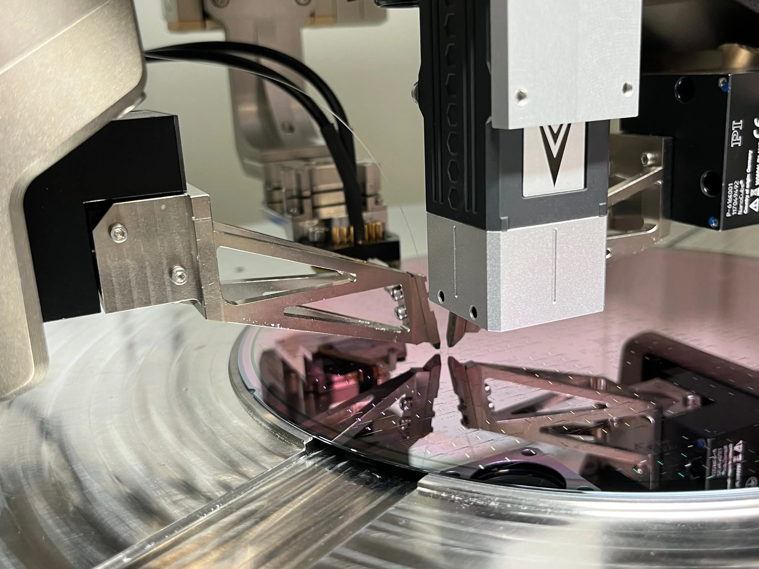
Wave Photonics enables new photonics fabrication processes to be rapidly brought online, especially those using novel materials or wavelengths targeting applications in sensing or quantum technologies.
Our core technology allows for the characterisation of a fabrication process and the subsequent rapid generation of a PDK of useable components at target wavelengths. The fabrication process can then be used to create functional chips without the difficulties and delays resulting from the coupled development of component designs and the fabrication process.

Process Design Kit (PDK)
A Process Design Kit (PDK) contains component designs and the information required to design a photonic chip. You can access the open-source PDK for the CORNERSTONE foundry, along with tutorials and component documentation for the powerful open-source layout software GDSFactory and L-Edit Photonics, a comprehensive photonics physical design environment developed by Siemens EDA. This should contain all of the information required to go from zero to laying out a chip design to be made as part of a cost-effective CORNERSTONE Multi-Project Wafer run.

QPICPAC - Chip Packaging Solution
As part of an Innovate UK project, QPICPAC, we have worked together with SENKO Advanced Components, a company producing high quality optical components, and Alter Technology, who offer advanced packaging solutions, to create an easy-to-use reusable packaging solution. Our packaging solution provides a template-driven approach to minimise custom development requirements and costs.